This is the Acorn 80 character by 25 line text card based on a 6845 type Cathode Ray Tube Controller (CRTC) chip. It provides all the timing and address signals.
The card is provided with 2K bytes of on-board RAM that stores the ASCII text to be displayed.
The pixel data for the characters is contained in an EPROM. It is text only so has no graphics capability.
Acorn intended it for use in "professional" applications.
It's normally found in System 5s. But can also be used in a System 3 or System 4.
This is another PCB from Chris Oddy. On this version he has made a minor change. It incorporates additional
circuitry to correct the Cursor and Dot Enable signals.
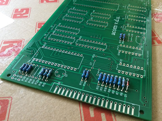
As normal, I have started by fitting the 1N4148 signal diodes and the resistors first.


Next up, the DIL sockets.


You may have spotted that I missed off one socket. Also one resistor is missing! I was building this card while attending an Acorn user meet-up called ABug South, that was being held at at The Ely, near, Blackwater, Camberley.
Needless to say, I had to bring all the parts with me, but I did not bring enough 82 ohm resistors. I'll correct this when I do some more work at home.
Well, I remembered ordering various tubes of DIL sockets from Rapid Electronics. But when I checked in my box of parts from Rapid, I found I had ordered 24 pin 0.3" sockets not the 24 pin 0.6" type that I needed...😞
Darn, another part that will have to wait until I get home. Hopefully I have some in stock.
But a little later, while I was looking through the bag of parts that I bought from ESR Electronic Components Ltd for another part (some ceramic capacitors), I discovered that I had ordered some 24 pin 0.6" sockets from them. Panic over 😂

Having added the 24 pin 0.6" socket, I continued by fitted the various capacitors, the single 2N2369A transistor and the pin headers for the various selection links.

The only bit that I find fiddly, is the two pin headers. It's just so
easy to solder them in, then turn the board over and find that the one
you have just done is wonky and leaning...

You may notice that I have not fitted the two presets (variable resistors) or some of the capacitors. That's because these form part of two "local" oscillators used for timing. I don't need these "local" oscillators because I'm using an Acorn 6502A CPU card. This version of the CPU card provides all the clock signals that this card needs, hence no need for any on-board "local" oscillators.
Time to dig into another box and grab the DIN 41612 AB 64-way connectors.

With that connector fitted, that's it for today. More soon.